22.4 ANALOG INPUTS AND OUTPUTS WITH CONTROLLOGIX
������������In this section analog I/O will be discussed using a 1794-IE4XOE2/B 4 Input/2Output 24V DC Non-Isolated Analog module. The card has a 12 bit resolution. To use this module it is defined under the 'I/O Configuration'. While configuring the module the following options are available.
After the card is configured the configuration words are available in the 'controller scooped tags'. These are listed below with descriptions assuming the card is in 'rack:2:'. The configuration words may also be used to update the card during operation. To do this the values are changed using normal program statements to read or write to values.
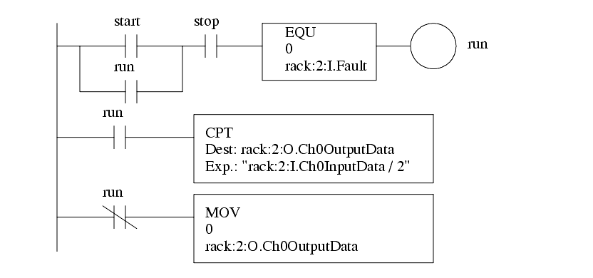
Figure 317 shows a simple analog IO example with some error checking. The system uses start and stop buttons to operate, along with a check for module errors. If the system is running the input voltage from input channel 0 will be divided by two and then set as the output voltage for output channel 0. If the system is not running the output voltage on channel zero is set to 0 (0V).
Although the card is a 12 bit card, it uses data values as if it has 15 digits of accuracy. Hence the valid range for the card is -32,768 to 32,767.
22.4.1 ANALOG INPUTS AND OUTPUTS WITH A PLC-5
������������(NOTE: This section is optional but is included for historical perspective.)
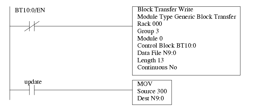
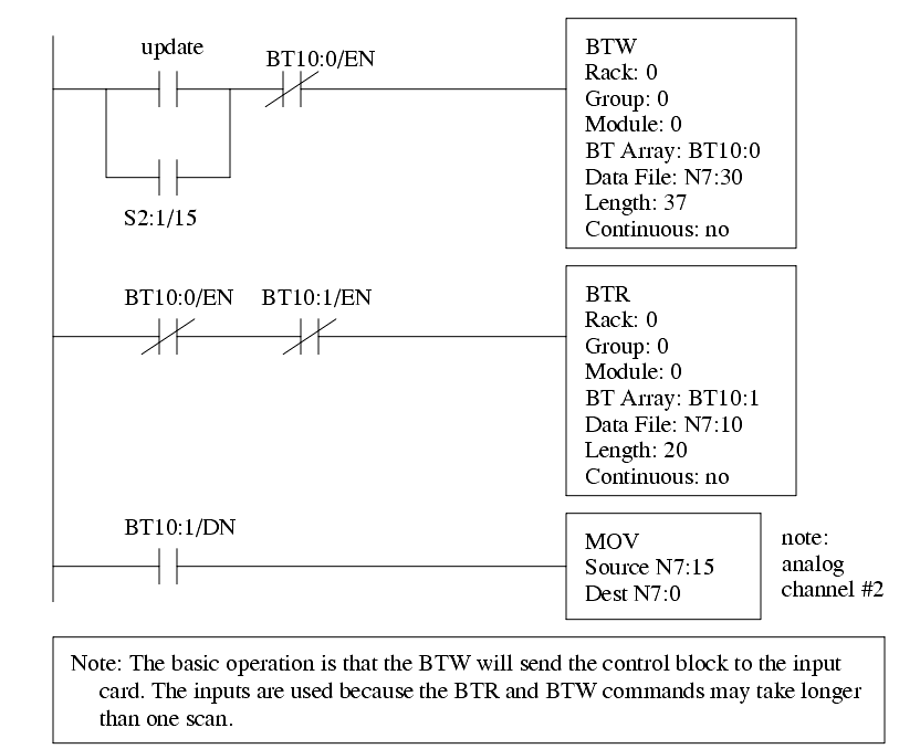
The PLC 5 ladder logic in Figure 318 will control an analog input card. The Block Transfer Write (BTW) statement will send configuration data from integer memory to the analog card in rack 0, slot 0. The data from N7:30 to N7:66 describes the configuration for different input channels. Once the analog input card receives this it will start doing analog conversions. The instruction is edge triggered, so it is run with the first scan, but the input is turned off while it is active, BT10:0/EN. This instruction will require multiple scans before all of the data has been written to the card. The update input is only needed if the configuration for the input changes, but this would be unusual. The Block Transfer Read (BTR) will retrieve data from the card and store it in memory N7:10 to N7:29. This data will contain the analog input values. The function is edge triggered, so the enable bits prevent it from trying to read data before the card is configured BT10:0/EN. The BT10:1/EN bit will prevent if from starting another read until the previous one is complete. Without these the instructions experience continuous errors. The MOV instruction will move the data value from one analog input to another memory location when the BTR instruction is done.
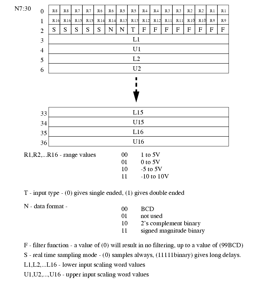
The data to configure a 1771-IFE Analog Input Card is shown in Figure 319. (Note: each type of card will be different, and you need to refer to the manuals for this information.) The 1771-IFE is a 12 bit card, so the range will have up to 2**12 = 4096 values. The card can have 8 double ended inputs, or 16 single ended inputs (these are set with jumpers on the board). To configure the card a total of 37 data words are needed. The voltage range of different inputs are set using the bits in word 0 (N7:30) and 1 (N7:31). For example, to set the voltage range on channel 10 to -5V to 5V we would need to set the bits, N7:31/3 = 1 and N7:31/2 = 0. Bits in data word 2 (N7:32) are set to determine the general configuration of the card. For example, if word 2 was 0001 0100 0000 0000b the card would be set for; a delay of 00010 between samples, to return 2s compliment results, using single ended inputs, and no filtering. The remaining data words, from 3 to 36, allow data values to be scaled to a new range. Words 3 and 4 are for channel 1, words 5 and 6 are for channels 2 and so on. To scale the data, the new minimum value is put in the first word (word 3 for channel 1), and the maximum value is put in the second word (word 4 for channel 1). The card then automatically converts the actual data reading between 0 and 4095 to the new data range indicated in word 3 and 4. One oddity of this card is that the data values for scaling must always be BCD, regardless of the data type setting. The manual for this card claims that putting zeros in the scaling values will cause the card to leave the data unscaled, but in practice it is better to enter values of 0 for the minimum and 4095 for the maximum.
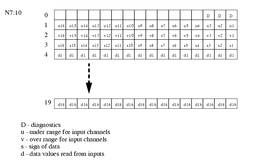
The block of data returned by the BTR statement is shown in Figure 320. Bits 0-2 in word 0 (N7:10) will indicate the status of the card, such as error conditions. Words 1 to 4 will reflect status values for each channel. Words 1 and 2 indicate if the input voltage is outside the set range (e.g., -5V to 5V). Word 3 gives the sign of the data, which is important if the data is not in 2s compliment form. Word 4 indicates when data has been read from a channel. The data values for the analog inputs are stored in words from 5 to 19. In this example, the status for channel 9 are N7:11/8 (under range), N7:12/8 (over range), N7:13/8 (sign) and N7:14/8 (data read). The data value for channel 9 is in N7:13.
Most new PLC programming software provides tools, such as dialog boxes to help set up the data parameters for the card. If these aids are not available, the values can be set manually in the PLC memory.
The PLC-5 ladder logic in Figure 321 can be used to set analog output voltages with a 1771-OFE Analog Output Card. The BTW instruction will write configuration memory to the card (the contents are described later). Values can also be read back from the card using a BTR, but this is only valuable when checking the status of the card and detecting errors. The BTW is edge triggered, so the BT10:0/EN input prevents the BTW from restarting the instruction until the previous block has been sent. The MOV instruction will change the output value for channel 1 on the card.
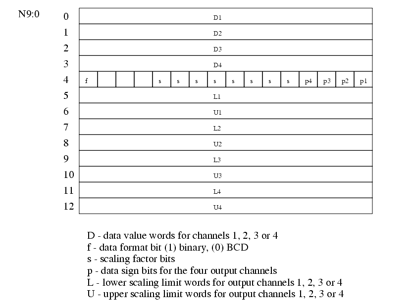
The configuration memory structure for the 1771-OFE Analog Output Card is shown in Figure 322. The card has four 12 bit output channels. The first four words set the output values for the card. Word 0 (N9:0) sets the value for channel 1, word 1 (N9:1) sets the value for channel 2, etc. Word 4 configures the card. Bit 16 (N9:4/15) will set the data format, bits 5 to 12 (/4 to /11) will enable scaling factors for channels, and bits 1 to 4 (/0 to /3) will provide signs for the data in words 0 to 3. The words from 5 to 13 allow scaling factors, so that the values in words 0 to 3 can be provided in another range of values, and then converted to the appropriate values. Good default values for the scaling factors are 0 for the lower limit and 4095 for the upper limit.
22.4.2 Pulse Width Modulation (PWM) Outputs
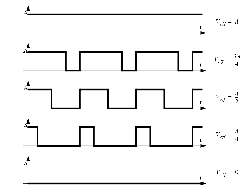
������������An equivalent analog output voltage can be generated using pulse width modulation, as shown in Figure 323. In this method the output circuitry is only capable of outputing a fixed voltage (in the figure 'A') or 0V. To obtain an analog voltage between the maximum and minimum the voltage is turned on and off quickly to reduce the effective voltage. The output is a square wave voltage at a high frequency, typically over 20Khz, above the hearing range. The duty cycle of the wave determines the effective voltage of the output. It is the percentage of time the output is on relative to the time it is off. If the duty cycle is 100% the output is always on. If the wave is on for the same time it is off the duty cycle is 50%. If the wave is always off, the duty cycle is 0%.
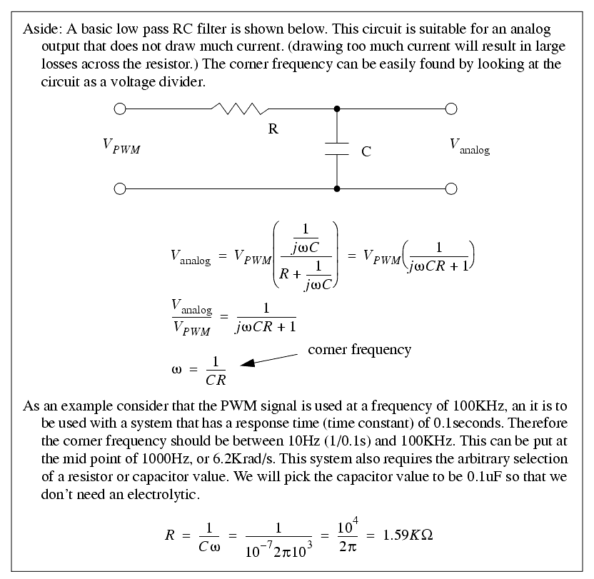
PWM is commonly used in power electronics, such as servo motor control systems. In this case the response time of the motor is slow enough that the motor effectively filters the high frequency of the signal. The PWM signal can also be put through a low pass filter to produce an analog DC voltage.
In some cases the frequency of the output is not fixed, but the duty cycle of the output is maintained.
22.4.3 Shielding
������������When a changing magnetic field cuts across a conductor, it will induce a current flow. The resistance in the circuits will convert this to a voltage. These unwanted voltages result in erroneous readings from sensors, and signal to outputs. Shielding will reduce the effects of the interference. When shielding and grounding are done properly, the effects of electrical noise will be negligible. Shielding is normally used for; all logical signals in noisy environments, high speed counters or high speed circuitry, and all analog signals.
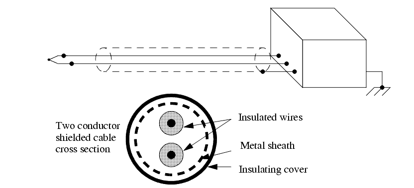
There are two major approaches to reducing noise; shielding and twisted pairs. Shielding involves encasing conductors and electrical equipment with metal. As a result electrical equipment is normally housed in metal cases. Wires are normally put in cables with a metal sheath surrounding both wires. The metal sheath may be a thin film, or a woven metal mesh. Shielded wires are connected at one end to "drain" the unwanted signals into the cases of the instruments. Figure 325 shows a thermocouple connected with a thermocouple. The cross section of the wire contains two insulated conductors. Both of the wires are covered with a metal foil, and final covering of insulation finishes the cable. The wires are connected to the thermocouple as expected, but the shield is only connected on the amplifier end to the case. The case is then connected to the shielding ground, shown here as three diagonal lines.
A twisted pair is shown in Figure 326. The two wires are twisted at regular intervals, effectively forming small loops. In this case the small loops reverse every twist, so any induced currents are cancel out for every two twists.

When designing shielding, the following design points will reduce the effects of electromagnetic interference.