Kirchoff’s voltage and current laws are shown in Figure 7.1 Kirchoff’s laws. The node current law holds true because the current flow in and out of a node must total zero. If the sum of currents was not zero then electrons would be appearing and disappearing at that node, thus violating the law of conservation of matter. The loop voltage law states that the sum of all rises and drops around a loop must total zero.
The simplest form of circuit analysis is for DC circuits, typically only requiring algebraic manipulation. In AC circuit analysis we consider the steady-state response to a sinusoidal input. Finally the most complex is transient analysis, often requiring integration, or similar techniques.
• DC (Direct Current) - find the response for a constant input.
• AC (Alternating Current) - find the steady-state response to an AC input.
• Transient - find the initial response to changes.
There is a wide range of components used in circuits. The simplest components are passive, such as resistors, capacitors and inductors. Active components are capable of changing their behaviors, such as op-amps and transistors. A list of components that will be discussed in this chapter are listed below.
• resistors - reduce current flow as described with ohm’s law
• voltage/current sources - deliver power to a circuit
• capacitors - pass current based on current flow, these block DC currents
• inductors - resist changes in current flow, these block high frequencies
• op-amps - very high gain amplifiers useful in many forms
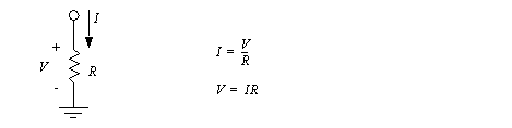
Resistance is a natural phenomenon found in all materials except superconductors. A resistor will oppose current flow as described by ohm’s law in Figure 7.2 Ohm’s law. The resistance value is assumed to be linear, but in actuality it varies with conductor temperature.
The voltage divider example in Figure 7.3 A voltage divider circuit illustrates the methods for analysis of circuits using resistors. In this circuit an input voltage is supplied on the left hand side. The output voltage on the right hand side will be some fraction of the input voltage. If the output resistance is very large, no current will flow, and the ratio of output to input voltages is determined by the ratio of the resistance between R1 and R2. To prove this the currents into the center node are summed and set equal to zero. The equations are then manipulated to produce the final relationship.
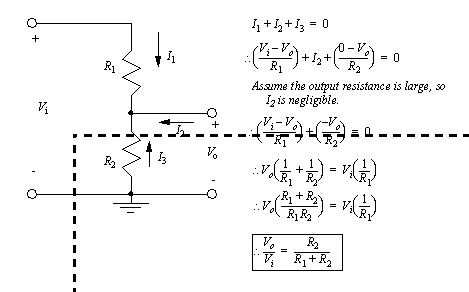
Figure 7.3 A voltage divider circuit
If two resistors are in parallel or series they can be replaced with a single equivalent resistance, as shown in Figure 7.4 Equivalent resistances for resistors in parallel and series.
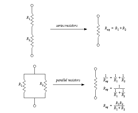
Figure 7.4 Equivalent resistances for resistors in parallel and series
A voltage source will maintain a voltage in a circuit, by varying the current as required. A current source will supply a current to a circuit, by varying the voltage as required. The schematic symbols for voltage and current sources are shown in Figure 7.5 Voltage and current sources. The supplies with ’+’ and ’-’ symbols provide DC voltages, with the symbols indicating polarity. The symbol with two horizontal lines is a battery. The circle with a sine wave is an AC voltage supply. The last symbol with an arrow inside the circle is a current supply. The arrow indicates the direction of positive current flow.
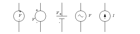
Figure 7.5 Voltage and current sources
A circuit containing a voltage source and resistors is shown in Figure 7.6 A circuit calculation. The circuit is analyzed using the node voltage method.
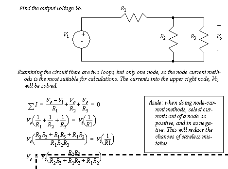
Figure 7.6 A circuit calculation
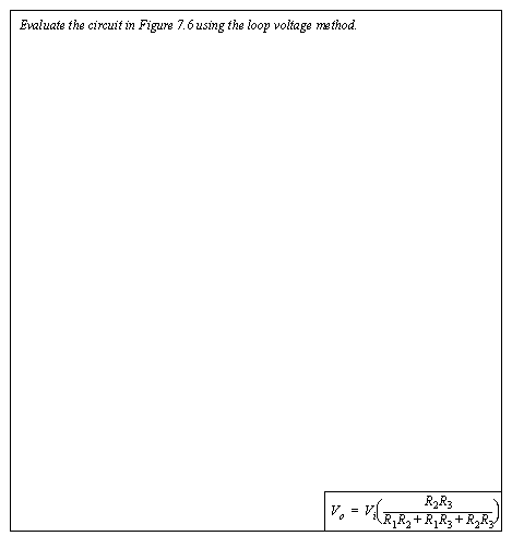
Figure 7.7 Drill problem: Mesh solution of voltage divider
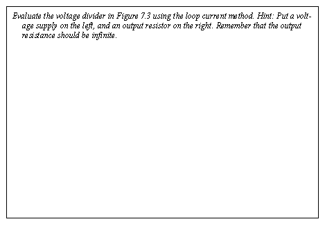
Figure 7.8 Drill problem: Mesh solution of voltage divider
Dependent (variable) current and voltage sources are shown in Figure 7.9 Dependent voltage sources. The voltage and current values of these supplies are determined by their relationship to some other circuit voltage or current. The dependent voltage source will be accompanied by a ’+’ and ’-’ symbol, while the current source has an arrow inside.
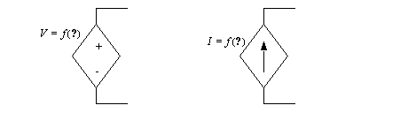
Figure 7.9 Dependent voltage sources
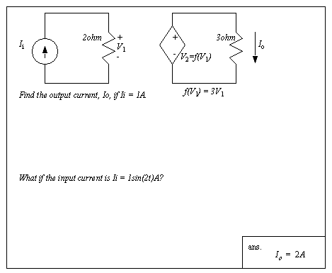
Figure 7.10 Drill problem: Find the currents in the circuit above
Capacitors are composed of two isolated metal plates very close together. When a voltage is applied across the capacitor, electrons will be forced into one plate, and forced out of the other plate. Temporarily this creates a small current flow until the plates reach equilibrium. So, any voltage change will result in some current flow. In practical terms this means that the capacitor will block any DC voltages, except for transient effects. But, high frequency AC currents will pass through the device. The equation for a capacitor and schematic symbols are given in Figure 7.11 Capacitors.
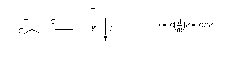
The symbol on the left is for an electrolytic capacitor. These contain a special fluid that increases the effective capacitance of the device but requires that the positive and negative sides must be observed in the circuit. (Warning: reversing the polarity on an electrolytic capacitor can make them leak, fail and possibly explode.) The other capacitor symbol is for a regular capacitor, normally with values under a microfarad.
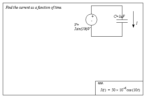
Figure 7.12 Drill problem: Current through a capacitor
While a capacitor will block a DC current, an inductor will pass it. Inductors are basically coils of wire. When a current flows through the coils, a magnetic field is generated. If the current through the inductor changes then the magnetic field must change, otherwise the field is maintained without effort (i.e., no voltage). Therefore the inductor resists changes in the current. The schematic symbol and relationship for an inductor are shown in Figure 7.13 An inductor.
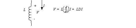
An inductor is normally constructed by wrapping wire in loops about a core. The core can be hollow, or be made of ferrite to increase the inductance. Inductors usually cost more than capacitors. In addition, inductors are susceptible to interference when metals or other objects disturb their magnetic fields. When possible, designers normally try to avoid using inductors in circuits.
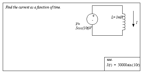
Figure 7.14 Drill problem: Current through an inductor
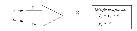
The ideal model of an op-amp is shown in Figure 7.15 An ideal op-amp. On the left hand side are the inverting and non-inverting inputs. Both of these inputs are assumed to have infinite impedance, and so no current will flow. Op-amp application circuits are designed so that the inverting and non-inverting inputs are driven to the same voltage level. The output of the op-amp is shown on the right. In circuits op-amps are used with feedback to perform standard operations such as those listed below.
• adders, subtractors, multipliers, and dividers - simple analog math operations
• amplifiers - increase the amplitude of a signal
• impedance isolators - hide the resistance of a circuit while passing a voltage
A simple op-amp example is given in Figure 7.16 A simple inverting operational amplifier configuration. As expected both of the op-amp input voltages are the same. This is a function of the circuit design. (Note: most op-amp circuits are designed to force both inputs to have the same voltage, so it is normally reasonable to assume they are the same.) The non-inverting input is connected directly to ground, so it will force both of the inputs to 0V. When the currents are summed at the inverting input, an equation including the input and output voltages is obtained. The final equation shows the system is a simple multiplier, or amplifier. The gain of the amplifier is determined by the ratio of the input and feedback resistors.
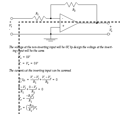
Figure 7.16 A simple inverting operational amplifier configuration
An op-amp circuit that can subtract signals is shown in Figure 7.17 Op-amp example.
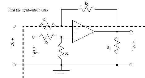
For ideal op-amp problems the node voltage method is normally the best choice. The equations for the circuit in Figure 7.17 Op-amp example are derived in Figure 7.18 Op-amp example (continued). The general approach to this solution is to sum the currents into the inverting and non-inverting input nodes. Notice that the current into the op-amp is assumed to be zero. Both the inverting and non-inverting input voltages are then set to be equal. After that, algebraic manipulation results in a final expression for the op-amp. Notice that if all of the resistor values are the same then the circuit becomes a simple subtractor.
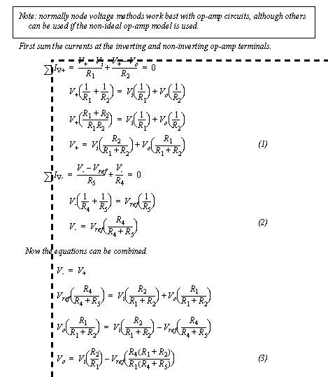
Figure 7.18 Op-amp example (continued)
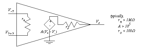
An op-amp (operational amplifier) has an extremely high gain, typically 100,000 times. The gain is multiplied by the difference between the inverting and non-inverting terminals to form an output. A typical op-amp will work for signals from DC up to about 100KHz. When the op-amp is being used for high frequencies or large gains, the model of the op-amp in Figure 7.19 A non-ideal op-amp model should be used. This model includes a large resistance between the inverting and non-inverting inputs. The voltage difference drives a dependent voltage source with a large gain. The output resistance will limit the maximum current that the device can produce, normally less than 100mA.