ANALOG INPUTSTo input an analog voltage (into a computer) the continuous voltage value must be sampled and then converted to a numerical value by an A/D (Analog to Digital) converter (also known as ADC). Figure 13.4 Sampling an Analog Voltage shows a continuous voltage changing over time. There are three samples shown on the figure. The process of sampling the data is not instantaneous, so each sample has a start and stop time. The time required to acquire the sample is called the sampling time. A/D converters can only acquire a limited number of samples per second. The time between samples is called the sampling period T, and the inverse of the sampling period is the sampling frequency (also called sampling rate). The sampling time is often much smaller than the sampling period. The sampling frequency is specified when buying hardware, but a common sampling rate is 100KHz. 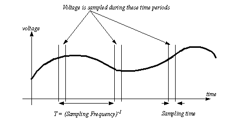
Figure 13.4 Sampling an Analog Voltage A more realistic drawing of sampled data is shown in Figure 13.5 Parameters for an A/D Conversion. This data is noisier, and even between the start and end of the data sample there is a significant change in the voltage value. The data value sampled will be somewhere between the voltage at the start and end of the sample. The maximum (Vmax) and minimum (Vmin) voltages are a function of the control hardware. These are often specified when purchasing hardware, but reasonable ranges are; The number of bits of the A/D converter is the number of bits in the result word. If the A/D converter is 8 bit then the result can read up to 256 different voltage levels. Most A/D converters have 12 bits, 16 bit converters are used for precision measurements. 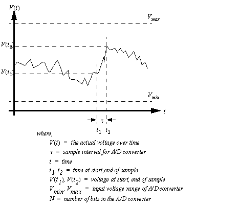
Figure 13.5 Parameters for an A/D Conversion The parameters defined in Figure 13.5 Parameters for an A/D Conversion can be used to calculate values for A/D converters. These equations are summarized in Figure 13.6 A/D Converter Equations. Equation 1 relates the number of bits of an A/D converter to the resolution. Equation 2 gives the error that can be expected with an A/D converter given the range between the minimum and maximum voltages, and the resolution (this is commonly called the quantization error). Equation 3 relates the voltage range and resolution to the voltage input to estimate the integer that the A/D converter will record. Finally, equation 4 allows a conversion between the integer value from the A/D converter, and a voltage in the computer. 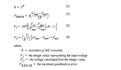
Figure 13.6 A/D Converter Equations Consider a simple example, a 10 bit A/D converter is set up to read voltages between -10V and 10V. This gives a resolution of 1024, where 0 is -10V and 1023 is +10V. Because there are only 1024 steps there is a maximum error of ±9.8mV. If a voltage of 4.564V is input, the A/D converter converts the voltage to an integer value of 746. When we convert this back to a voltage the result is 4.570V. The resulting quantization error is 4.570V-4.564V=+0.006V. This error can be reduced by selecting an A/D converter with more bits. Each bit halves the quantization error. 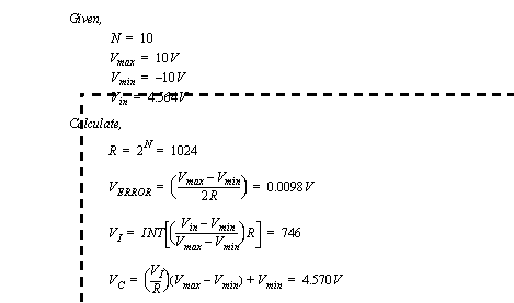
Figure 13.7 Sample Calculation of A/D Values If the voltage being sampled is changing too fast we may get false readings, as shown in Figure 13.8 Low Sampling Frequencies Cause Aliasing. In the upper graph the waveform completes seven cycles, and 9 samples are taken. The bottom graph plots out the values read. The sampling frequency was too low, so the signal read appears to be different than it actually is, this is called aliasing. 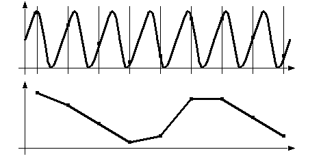
Figure 13.8 Low Sampling Frequencies Cause Aliasing 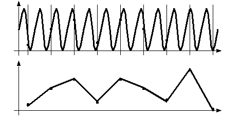
Figure 13.9 Very Low Sampling Frequencies Produce Apparently Random The Nyquist criterion specifies that sampling frequencies should be at least twice the frequency of the signal being measured, otherwise aliasing will occur. The example in Figure 13.8 Low Sampling Frequencies Cause Aliasing violated this principle, so the signal was aliased. If this happens in real applications the process will appear to operate erratically. In practice the sample frequency should be 4 or more times faster than the system frequency. 
There are other practical details that should be considered when designing applications with analog inputs; • Noise - Since the sampling window for a signal is short, noise will have added effect on the signal read. For example, a momentary voltage spike might result in a higher than normal reading. Shielded data cables are commonly used to reduce the noise levels. • Delay - When the sample is requested, a short period of time passes before the final sample value is obtained. • Multiplexing - Most analog input cards allow multiple inputs. These may share the A/D converter using a technique called multiplexing. If there are 4 channels using an A/D converter with a maximum sampling rate of 100Hz, the maximum sampling rate per channel is 25Hz. • Signal Conditioners - Signal conditioners are used to amplify, or filter signals coming from transducers, before they are read by the A/D converter. • Resistance - A/D converters normally have high input impedance (resistance), so they affect circuits they are measuring. • Single Ended Inputs - Voltage inputs to the A/D converter can use a single common for multiple inputs, these types of inputs are called single ended inputs. These tend to be more prone to noise. • Double Ended Inputs - Each double ended input has its own common. This reduces problems with electrical noise, but also tends to reduce the number of inputs by half. • Sampling Rates - The maximum number of samples that can be read each second. If reading multiple channels with a multiplexer, this may be reduced. • Quantization Error - Analog IO is limited by the binary resolution of the converter. This means that the output is at discrete levels, instead of continuous values. • Triggers - often external digital signals are used to signal the start of data collection. • Range - the typical voltages that the card can read. Typical voltage ranges are -10V to 10V, 0V to 10V, 0V to 5V, 1V to 5V, -5V to 5V, 4mA to 20mA. • DMA - a method to write large blocks of memory directly to computer memory. This is normally used for high speed data captures. • Filters - some A/D input cards will provide built in functions to filter the incoming data to remove high frequency noise components. • Input impedance - most analog inputs have very high input resistances, in the range of Mohms. 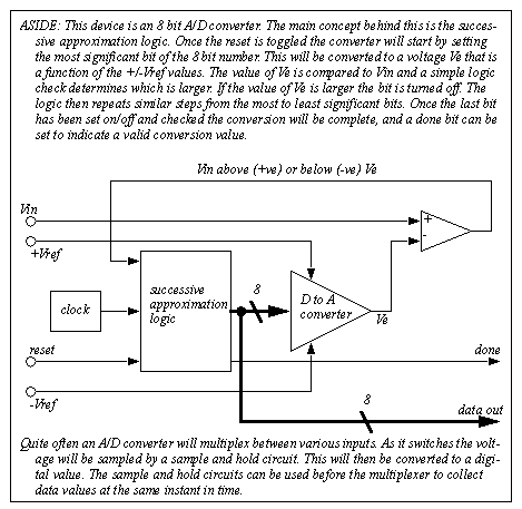
|