1.5 SELECTION OF ELECTRICAL COMPONENTS
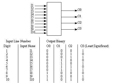
Up to this point the examples have been mainly limited to discrete manufacturing of mechanical parts. In this section a somewhat novel approach of the planner will be suggested. This is given for some illustration of the implications of this planning approach. The example chosen was a digital circuit design for an encoder that would take ten input lines, and derive a four bit binary output number that would indicate which of the input lines is active. The design was done in a format similar to the previous designs, except that obvious features such as geometrical features are no longer needed.
The digital-to-binary encoder is a simple logical circuit using combinatorial logic expressions. The truth table for such a system is shown below.
Figure 1.1 Truth Table for Digital to Binary Encoder
This can be directly converted to as design file, as shown below.
// This is a description of a digital circuit that does 10 bit digital
// input to 4 bit binary output conversion
main decade_to_binary {
EQUATION: ( : A B C D )
}
A {
// The least significant bit
EQUATION: ( + I1 I3 I5 I7 I9 )
}
B {
// The second least significant bit
EQUATION: ( + I2 I3 I6 I7 I10 )
}
Figure 1.2 A Product Description File for a Digital to Binary Encoder
C {
// The second most significant bit
EQUATION: ( + I4 I5 I6 I7 )
}
D {
// The most significant bit
EQUATION: ( + I8 I9 I10 )
}
I1 {
// input for 0
form = INPUT
}
I2 {
// input for 1
form = INPUT
}
I3 {
// input for 2
form = INPUT
}
I4 {
// input for 3
form = INPUT
}
I5 {
// input for 4
form = INPUT
}
I6 {
// input for 5
form = INPUT
}
I7 {
// input for 6
form = INPUT
}
I8 {
// input for 7
form = INPUT
}
I9 {
// input for 8
form = INPUT
}
I10 {
// input for 9
form = INPUT
}
A Product Description File for a Digital to Binary Encoder (cont’d)
The file above is sufficient to describe the function of the circuit. Interesting is the representation of the parallel Boolean equations using the assembly operator that is not often used in standard switching circuit design theory. This design was then planned with a set of rules shown below.
// Rules for selecting chips for digital circuits
// The equation templates are listed here
equation_form 2_INPUT_OR_GATES {
EQUATION: ( + VAR:V:0 VAR:V:1 ...)
RULE: 2_input_or
}
equation_form 3_INPUT_OR_GATES {
EQUATION: ( + VAR:V:0 VAR:V:1 VAR:V:2 ...)
RULE: 3_input_or
}
equation_form 4_INPUT_OR_GATES {
EQUATION: ( + VAR:V:0 VAR:V:1 VAR:V:2 VAR:V:3 ...)
RULE: 4_input_or
}
equation_form FIND_SINGLE_TERM_OR {
EQUATION: ( + VAR:V:0 )
RULE: Eliminate_single_term
}
equation_form OUTPUT_LIST {
EQUATION: (> : VAR:V:0 ...)
RULE: List_output_connection
}
// The rules are listed here
rule 2_input_or {
EQUATION: ( & ( + 1_INPUT 1_RESULTANT ) ( + 2_INPUT
2_RESULTANT ) )
RESULT: USE_2_INPUT_OR_GATE
}
rule 3_input_or {
EQUATION: ( & ( + 1_INPUT 1_RESULTANT ) ( + 2_INPUT 2_RESULTANT )
( + 3_INPUT 3_RESULTANT ) )
RESULT: USE_3_INPUT_OR_GATE
}
rule 4_input_or {
EQUATION: ( & ( + 1_INPUT 1_RESULTANT ) ( + 2_INPUT 2_RESULTANT )
( + 3_INPUT 3_RESULTANT ) ( + 4_INPUT 4_RESULTANT ) )
RESULT: USE_4_INPUT_OR_GATE
}
Figure 1.1 Rules For Converting a Digital Design to Gate Embodiment
rule List_output_connection {
EQUATION: ( & 1_EXISTS )
RESULT: ADD_OUTPUT_TO_LIST
}
rule Eliminate_single_term {
EQUATION: ( & 1_EXISTS )
RESULT: KILL_SINGLE_TERM
}
// The rule conditions are used here
condition 1_EXISTS {
COMPARE ( V0.form $ )
}
condition 1_INPUT {
COMPARE ( V0.form $ )
COMPARE ( V0.form == INPUT )
}
condition 1_RESULTANT {
COMPARE ( V0.form $ )
COMPARE ( V0.form == CALCULATED )
}
condition 2_INPUT {
COMPARE ( V1.form $ )
COMPARE ( V1.form == INPUT )
}
condition 2_RESULTANT {
COMPARE ( V1.form $ )
COMPARE ( V1.form == CALCULATED )
}
condition 3_INPUT {
COMPARE ( V2.form $ )
COMPARE ( V2.form == INPUT )
}
condition 3_RESULTANT {
COMPARE ( V2.form $ )
COMPARE ( V2.form == CALCULATED )
}
condition 4_INPUT {
COMPARE ( V3.form $ )
COMPARE ( V3.form == INPUT )
}
condition 4_RESULTANT {
COMPARE ( V3.form $ )
COMPARE ( V3.form == CALCULATED )
}
// The rule results are defined here
result USE_2_INPUT_OR_GATE {
COPY_SET ( V0 2_INPUT_GATE )
FIND ( 2_INPUT_GATE input_0 SET_NAME V0 )
Rules For Converting a Digital Design to Gate Embodiment (cont’d)
FIND ( 2_INPUT_GATE input_1 SET_NAME V1 )
EQUATION_INSERT_SYMBOL ( :0 2_INPUT_GATE )
EQUATION_DELETE_SYMBOL ( :1 )
EQUATION_DELETE_SYMBOL ( :1 )
DELETE_PROPERTY ( 2_INPUT_GATE form )
ADD_PROPERTY ( 2_INPUT_GATE form = CALCULATED )
ADD_PROPERTY ( 2_INPUT_GATE cost = 0.50 )
DECLARE_COST ( 2_INPUT_GATE cost )
PLAN_PUSH_FORMAT ( ‘ DESCRIPTION ( Use 2 input OR gate for ‘
2_INPUT_GATE.input_0 2_INPUT_GATE.input_1 ‘ ) ‘ )
DELETE_PROPERTY ( 2_INPUT_GATE input_0 )
DELETE_PROPERTY ( 2_INPUT_GATE input_1 )
FIND ( 2_INPUT_GATE output THIS_NAME 2_INPUT_GATE )
PLAN_PUSH_FORMAT ( ‘ DESCRIPTION ( Output is ‘
2_INPUT_GATE.output ‘ ) ‘ )
DELETE_PROPERTY ( 2_INPUT_GATE output )
}
result USE_3_INPUT_OR_GATE {
COPY_SET ( V0 3_INPUT_GATE )
FIND ( 3_INPUT_GATE input_0 SET_NAME V0 )
FIND ( 3_INPUT_GATE input_1 SET_NAME V1 )
FIND ( 3_INPUT_GATE input_2 SET_NAME V2 )
EQUATION_INSERT_SYMBOL ( :0 3_INPUT_GATE )
EQUATION_DELETE_SYMBOL ( :1 )
EQUATION_DELETE_SYMBOL ( :1 )
EQUATION_DELETE_SYMBOL ( :1 )
DELETE_PROPERTY ( 3_INPUT_GATE form )
ADD_PROPERTY ( 3_INPUT_GATE form = CALCULATED )
ADD_PROPERTY ( 3_INPUT_GATE cost = 0.65 )
DECLARE_COST ( 3_INPUT_GATE cost )
PLAN_PUSH_FORMAT ( ‘ DESCRIPTION ( Use 3 input OR gate for ‘
3_INPUT_GATE.input_0 3_INPUT_GATE.input_1 3_INPUT_GATE.input_2
‘ ) ‘ )
DELETE_PROPERTY ( 3_INPUT_GATE input_0 )
DELETE_PROPERTY ( 3_INPUT_GATE input_1 )
DELETE_PROPERTY ( 3_INPUT_GATE input_2 )
FIND ( 3_INPUT_GATE output THIS_NAME 3_INPUT_GATE )
PLAN_PUSH_FORMAT ( ‘ DESCRIPTION ( Output is ‘
3_INPUT_GATE.output ‘ ) ‘ )
DELETE_PROPERTY ( 3_INPUT_GATE output )
}
result USE_4_INPUT_OR_GATE {
COPY_SET ( V0 4_INPUT_GATE )
FIND ( 4_INPUT_GATE input_0 SET_NAME V0 )
FIND ( 4_INPUT_GATE input_1 SET_NAME V1 )
FIND ( 4_INPUT_GATE input_2 SET_NAME V2 )
FIND ( 4_INPUT_GATE input_3 SET_NAME V3 )
EQUATION_INSERT_SYMBOL ( :0 4_INPUT_GATE )
EQUATION_DELETE_SYMBOL ( :1 )
EQUATION_DELETE_SYMBOL ( :1 )
Rules For Converting a Digital Design to Gate Embodiment (cont’d)
EQUATION_DELETE_SYMBOL ( :1 )
DELETE_PROPERTY ( 4_INPUT_GATE form )
ADD_PROPERTY ( 4_INPUT_GATE form = CALCULATED )
ADD_PROPERTY ( 4_INPUT_GATE cost = 0.75 )
DECLARE_COST ( 4_INPUT_GATE cost )
PLAN_PUSH_FORMAT ( ‘ DESCRIPTION ( Use 4 input OR gate for ‘
4_INPUT_GATE.input_0 4_INPUT_GATE.input_1 4_INPUT_GATE.input_2
4_INPUT_GATE.input_3 ‘ ) ‘ )
DELETE_PROPERTY ( 4_INPUT_GATE input_0 )
DELETE_PROPERTY ( 4_INPUT_GATE input_1 )
DELETE_PROPERTY ( 4_INPUT_GATE input_2 )
DELETE_PROPERTY ( 4_INPUT_GATE input_3 )
}
result ADD_OUTPUT_TO_LIST {
COPY_SET ( V0 OUTPUT )
FIND ( OUTPUT output SET_NAME V0 )
EQUATION_DELETE_SYMBOL ( :0 )
ADD_PROPERTY ( OUTPUT form = CALCULATED )
ADD_PROPERTY ( OUTPUT cost = 0.05 )
DECLARE_COST ( OUTPUT cost )
PLAN_PUSH_FORMAT ( ‘ DESCRIPTION ( Connect output for ‘
OUTPUT.output ‘ ) ‘ )
}
result KILL_SINGLE_TERM {
COPY_SET ( V0 OUTPUT )
FIND ( OUTPUT output SET_NAME V0 )
FIND ( OUTPUT terminal THIS_PART )
EQUATION_DELETE_SYMBOL ( :0 )
PLAN_PUSH_FORMAT ( ‘ DESCRIPTION ( Connect gate output ‘
OUTPUT.output ‘ to output ‘ OUTPUT.terminal ‘ ) ‘ )
}
Rules For Converting a Digital Design to Gate Embodiment (cont’d)
For the sake of brevity, the rules only used OR gates, but these are sufficient to implement the design. These rules were applied to the design to get the following process plan for connecting the circuit.
-------- Work Order Sheets ------------
Product: decade_to_binary
OPERATION SUMMARY_SHEET: D_PART - Quantity 1.000000
OP# Operation Description
------------------------------------------
0 Connect gate output 2_INPUT_GATE_5 to output D_OP5
10 Use 2 input OR gate for 2_INPUT_GATE_3 I10
Output is 2_INPUT_GATE_5
20 Use 2 input OR gate for I8 I9
Output is 2_INPUT_GATE_3
OPERATION SUMMARY_SHEET: C_PART - Quantity 1.000000
OP# Operation Description
------------------------------------------
1000 Connect gate output 2_INPUT_GATE_12 to output C_OP12
1010 Use 2 input OR gate for 2_INPUT_GATE_10 I7
Output is 2_INPUT_GATE_12
1020 Use 2 input OR gate for 2_INPUT_GATE_8 I6
Output is 2_INPUT_GATE_10
1030 Use 2 input OR gate for I4 I5
Output is 2_INPUT_GATE_8
OPERATION SUMMARY_SHEET: B_PART - Quantity 1.000000
OP# Operation Description
------------------------------------------
2000 Connect gate output 2_INPUT_GATE_21 to output B_OP21
2010 Use 2 input OR gate for 2_INPUT_GATE_19 I10
Output is 2_INPUT_GATE_21
2020 Use 2 input OR gate for 2_INPUT_GATE_17 I7
Output is 2_INPUT_GATE_19
2030 Use 2 input OR gate for 2_INPUT_GATE_15 I6
Output is 2_INPUT_GATE_17
2040 Use 2 input OR gate for I2 I3
Output is 2_INPUT_GATE_15
OPERATION SUMMARY_SHEET: A_PART - Quantity 1.000000
OP# Operation Description
------------------------------------------
3000 Connect gate output 2_INPUT_GATE_30 to output A_OP30
3010 Use 2 input OR gate for 2_INPUT_GATE_28 I9
Output is 2_INPUT_GATE_30
3020 Use 2 input OR gate for 2_INPUT_GATE_26 I7
Output is 2_INPUT_GATE_28
3030 Use 2 input OR gate for 2_INPUT_GATE_24 I5
Output is 2_INPUT_GATE_26
3040 Use 2 input OR gate for I1 I3
Output is 2_INPUT_GATE_24
OPERATION SUMMARY_SHEET: decade_to_binary_PART - Quantity 1.000000
OP# Operation Description
------------------------------------------
4000 Connect output for D_PART
4010 Connect output for C_PART
4020 Connect output for B_PART
4030 Connect output for A_PART
Figure 1.1 A Process Plan for Circuit Construction
This process plan is a bit naive, but it does allow construction of the part automatically. Some points of interest in this case are,
- the operations to produce the part are reversed. This is not a large problem, but indicates that some problems are not necessarily suited to backwards planning,
- two input OR gates have been chosen, as opposed to 3 or 4 input gates. This is the result of a search routine that only considers the cheapest operation first. A more extensive search routine would do a more cost based approach to planning,
- the system was easily able to track inputs and outputs to gates, and generate unique identifiers to minimize confusion.
This example illustrates that the BCAPP approach is truly multi-domain, and is able to be extended to a number of problems.